Are you struggling to understand FPGA design flow? If so, you're not alone. Many newcomers find it confusing. The design flow involves several steps, and first-time users often feel overwhelmed. Whether you're a hobbyist or a professional, having a clear understanding can help you use FPGA boards effectively. In this guide, we will clarify this process and help you avoid common pitfalls in FPGA
Are you struggling to understand FPGA design flow? If so, you're not alone. Many newcomers find it confusing. The design flow involves several steps, and first-time users often feel overwhelmed. Whether you're a hobbyist or a professional, having a clear understanding can help you use FPGA boards effectively. In this guide, we will clarify this process and help you avoid common pitfalls in FPGA design. We’ll cover essential terms and tools related to FPGA development.
The FPGA design flow is a sequence of steps that involve specification, design, implementation, and verification. This process is essential to develop effective FPGA solutions. Understanding each step will lead to better FPGA board performance and results.
The specification stage is critical. For example, a designer may specify a digital filter for audio processing. They must list performance criteria such as frequency response, noise level, and delay. This foundation helps streamline the later stages of the design flow.
Consider a simple counter. The designer writes code in VHDL to describe how the counter behaves. They define inputs, outputs, and the operation—like incrementing the count on each clock pulse. This step links user requirements with practical implementation.
| Step | Description | Tools |
|---|---|---|
| 1 | Specification: Outline requirements | Text Documents |
| 2 | Design Entry: Write HDL Code | VHDL, Verilog |
| 3 | Synthesis: Convert code to logic | Synthesis Tools |
| 4 | Implementation: Map to FPGA architecture | Implementation Tools |
| 5 | Verification: Ensure design meets specs | Simulation Tools |
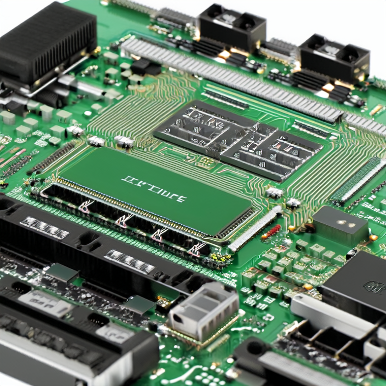
After synthesis, the next step is to implement your design. This means mapping it onto the specific architecture of the FPGA board. Successfully doing this requires knowledge of the board's resources, such as logic elements, memory blocks, and routing circuits.
Understanding the FPGA design flow is vital for both beginners and more experienced users. By breaking down the steps, anyone can grasp how to approach FPGA board projects. From specifying your project needs to verifying final designs, each step is important. Mastering this flow will enable you to build better FPGA solutions successfully.
FPGA stands for Field-Programmable Gate Array. It is a type of hardware that can be programmed to perform specific tasks.
Yes, you can use languages like VHDL and Verilog to describe your design for FPGA boards.
Synthesis can be challenging as it requires accurate conversion of high-level languages into a format that FPGAs can use.